All DataSheet
Home » Linear » LTC6081CDD DataSheet
LTC6081CDD DataSheet

LTC6081CDD DataSheet

Part No.
LTC6081CDD
Part Marking
LCJP
Temperature
0°C to 70°C
Package
10-Lead (3mm × 3mm) Plastic DFN
File Size
276 KB
Page
20 Pages
Manufacturer
Linear Technology
Views
1
Upload Time
2022-07-01 12:03:21
Update Time
2022-07-01
Description
IC CMOS 2 CIRCUIT 10DFN
If you would like to buy it now or in the future, please email or add our skype hello@ic-component.com

LTC6081CDD Features

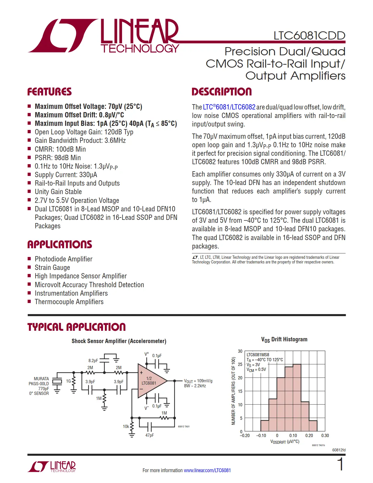
■ Maximum Offset Voltage: 70μV (25°C)
■ Maximum Offset Drift: 0.8μV/°C
■ Maximum Input Bias: 1pA (25°C) 40pA (TA ≤ 85°C)
■ Open Loop Voltage Gain: 120dB Typ
■ Gain Bandwidth Product: 3.6MHz
■ CMRR: 100dB Min
■ PSRR: 98dB Min
■ 0.1Hz to 10Hz Noise: 1.3μVP-P
■ Supply Current: 330μA
■ Rail-to-Rail Inputs and Outputs
■ Unity Gain Stable
■ 2.7V to 5.5V Operation Voltage
■ Dual LTC6081 in 8-Lead MSOP and 10-Lead DFN10
■ Packages; Quad LTC6082 in 16-Lead SSOP and DFN Packages

LTC6081CDD Applications

■ Photodiode Amplifier
■ Strain Gauge
■ High Impedance Sensor Amplifier
■ Microvolt Accuracy Threshold Detection
■ Instrumentation Amplifiers
■ Thermocouple Amplifiers

LTC6081CDD Description

The LTC6081CDD are dual/quad low offset, low drift, low noise CMOS operational amplifiers with rail-to-rail input/output swing.

The 70μV maximum offset, 1pA input bias current, 120dB open loop gain and 1.3μVP-P 0.1Hz to 10Hz noise make it perfect for precision signal conditioning. The LTC6081CDD features 100dB CMRR and 98dB PSRR.

Each amplifier consumes only 330μA of current on a 3V supply. The 10-lead DFN has an independent shutdown function that reduces each amplifier’s supply current to 1μA.

LTC6081CDD is specified for power supply voltages of 3V and 5V from –40°C to 125°C. The dual LTC6081 is available in 8-lead MSOP and 10-lead DFN10 packages.

Related LTC6081CDD Datasheet

Part No.
Datasheet

276Kb / 20P

276Kb / 20P

276Kb / 20P

276Kb / 20P

CopyRight © 2022 All DataSheet(www.all-datasheet.com)TXTLTADI